Company History
1976
December
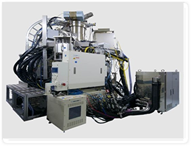
Transfer of semiconductor manufacturing equipment business technology, centered on electronic beam mask writers, from Toshiba Corporation to Toshiba Machine Co., Ltd. (currently NuFlare Technology).
An electronic beam mask writer-related technical support agreement was signed between Toshiba Corporation and Toshiba Machine Co., Ltd. (currently NuFlare Technology), and the development, manufacturing, and ordering of the EBM-105 series writers commenced, based on the collaboration of Toshiba Corporation.
1979
April
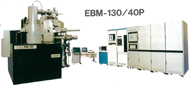
Electronic beam mask writer won the Nikkan Kogyo Shimbun newspaper's Best 10 New Products Prize*1
(*1 Every year, the Nikkan Kogyo Shimbun newspaper carefully selects and recognizes ten excellent items from among products developed and commercialized by Japanese corporations.)
1984
June
Through a joint project with Toshiba Corporation's research laboratory, completed a variable shaped beam-type electronic beam mask writer (EBM-130V), our first model.
1992
June
With Toshiba Corporation, jointly developed the HT-2000 (carbon heating-type) high-speed rotating epitaxial growth system. This was Japan's first domestically produced sheet system.
1994
December
Developed and commercialized HT2000B Epitaxial Reactor.
1995
December
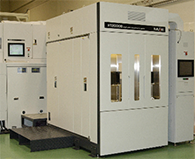
Received The Prize for the Promotion of the Machine Industry
1998
December
Through a joint project with Toshiba Corporation, developed and commercialized a variable shaped beam-type electronic beam mask writer (EBM-3000). Our first commercial model, this was compatible with 180-150nm design rules.
2002
June
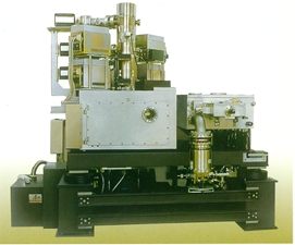
Developed and commercialized EBM-4000 EB Mask Writer for 90-nm (circuit line) design rules. (Up to this point, Semiconductor Equipment Division of Toshiba Machine Co., Ltd.).
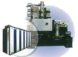
June
Developed and commercialized HT3000 12 Single Wafer Si Epitaxial Reactor.
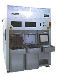
August
NuFlare Technology, Inc. took over the entire semiconductor equipment business of Toshiba Machine Co., Ltd. and commenced operations.
December
Participated in Semicon Japan 2002 for the first time as NuFlare Technology, Inc.
2003
February
Expansion of clean room as manufacturing facilities expanded.
April
Development commissioning agreement signed with Toshiba Machine Company, America, the US subsidiary of Toshiba Machine Co., Ltd., and the USA Satellite office established.
November
Opened the "Yokohama Satellite" office, an R&D base, in Yokohama. (In October 2004, moved Sales Division to Yokohama Satellite.)
2004
September
Developed and commercialized EBM-5000 electron beam mask writer for 65-nm circuit lines.
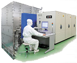
November
In recognition of development of proximity effect compensation technology, awarded the Promotion Foundation for Electrical Science and Engineering Award*2 (Ohm Technology Award), a special prize to commemorate the 90th anniversary of the foundation of Ohmsha, Ltd. (*2 The Promotion Foundation for Electrical Science and Engineering confers this prize on an organization or individual who has achieved excellent results and is expected to achieve still more outstanding results in the future fors an invention, modification, production increase, research, or survey, etc., that has contributed to the advance of Japan's electrical technology or the development of electrical utilities industries, telecommunications, or electronic communications culture.)
2006
March
Reception of Intel's "Preferred Quality Supplier"(PQS) Award
April
Announcment of EBM-6000
June
Mask Inspection Business started
2007
March
Started-up Yokohama Operations
April
Equity listed on JASDAQ Securities Exchange
October
NuFlare Technology headquarters relocate to Shinyokohama, Kouhoku-ku Yokohama-shi Kanagawa.
2008
February
Developed and commercialized EBM-6000PLUS (for double patterning research and development).
March
Developed and commercialized EBM-7000 (for half-pitch (hp) 32 nm node generation).
2009
March
Established NFT KOREA,Inc. in Suwon,Korea
2010
April
Equity listed on Osaka Securities Exchange JASDAQ Standard due to Osaka Securities Exchange merged with Jasdaq Securities Exchange, Inc.
2011
August
Developed and commercialized EBM-8000 (for 14 nm technology node, half-pitch (hp) 22 nm node generation).
2013
February
NuFlare Awarded The 59th Okochi Memorial Grand Production Prize
May
Developed and commercialized EBM-9000 (for 10 nm technology node).
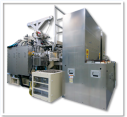
June
Opened NFT Germany Branch Office in Dresden, Germany.
July
Equity listed on Tokyo Stock Exchange JASDAQ Standard due to Tokyo Stock Exchange merged with Osaka Securities Exchange.
October
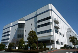
NuFlare Technology headquarters relocate to Shinsugita, isogo-ku Yokohama-shi Kanagawa.
November
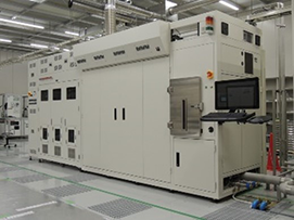
Released EPIREVOTM G8 GaN-on-Si MOCVD for LED on 8 silicone substrates.
2014
January
Established NuFlare Technology America, Inc.
August
Developed and commercialized EPIREVOTM S6 SiC Epitaxial Reactor.
2015
July
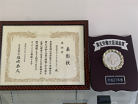
Won the Incentive Award for Safety Award by Minister of Health, Labour and Welfare
August
Developed and commercialized EBM-9500 (for 7 nm technology node).
2019
July
Developed and commercialized EBM-9500PLUS (for 5nm/7nm+ nm technology node).
Developed and commercialized EBM-8000P (for 14/16 nm technology node, 20~45 nm technology node ).
October
Established NFT Taiwan, Inc. (the company’s Taiwan subsidiary) NFT Taiwan, Inc.
2020
March
Delisted from Tokyo Stock Exchange as of March 30,2020
April
Toshiba Electronic Devices & Storage Corporation acquired 100% shares of NuFlare Technology, Inc. as a subsidiary company.
June
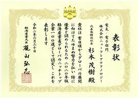
Selected as one of the “Global Niche Top 100 Companies” by the Ministry of Economy, Trade and Industry.
2021
October
Developed and commercialized EPIREVOTM S8 SiC Epitaxial Reactor.
2022
March
Developed and commercialized MBM™-2000 (for 3nm technology node generation).
